
1- Introduction
The rapid growth of mobile computing, AI, and Automotive technologies is driving demand for faster, more efficient, and highly reliable memory with higher capacity. Initially built for mobile devices, LPDDR5/4 has evolved into a critical enabler for high-bandwidth, high-capacity, low-power applications across AI, Automotive, and High-Performance Computing.
LPDDR5X marks a major leap, delivering higher data rates, higher capacity, lower latency, and greater power efficiency, which is ideal for AI workloads, advanced mobile devices, ADAS, and automotive infotainment. Reaching up to 10.7 Gbps, it offers the performance and capacity needed for real-time data processing with minimal power consumption. Capable of delivering a 16GB total capacity with 32-bit Data width (DQ), LPDDR5X positions itself as a strong choice for applications where speed, capacity, and form factor are crucial requirements.
As older LPDDR generations approach end-of-life, LPDDR5X stands out as a cost-effective, widely available, and scalable solution for future-ready designs. This white paper examines LPDDR5X’s evolution, benefits, and real-world applications, while showcasing how Innosilicon’s latest 10.7 Gbps LPDDR5X Combo IP is enabling breakthrough innovation across industries.
2- LPDDR5X: The Evolution of High-Performance Memory
Exceptional Data Rates
LPDDR (Low Power Double Data Rate) memory has evolved rapidly to meet growing demands for higher speed, lower power, and greater efficiency. Originally developed for mobile devices, LPDDR has expanded into automotive, AI, and high-performance computing. Beginning with LPDDR1 in the early 2000s, each generation of LPDDR2, LPDDR3, and LPDDR4 brought improvements in data rates and power optimization. LPDDR4X further enhanced bandwidth and energy efficiency, supporting high-resolution displays and multi-camera systems.
The introduction of LPDDR5 in 2019 marked a major leap, delivering up to 6400Mbps and adding features like in-line ECC for improved reliability. The latest advancement, LPDDR5X, reaches speeds up to 10.7 Gbps with lower latency, better signal integrity, and greater
power savings. LPDDR5X is offering a speed that is 2.5X compared to LPDDR4X, which is a key enabler for AI inference, ADAS, Robotics, and next-gen mobile applications, where real-time processing and energy efficiency are critical.
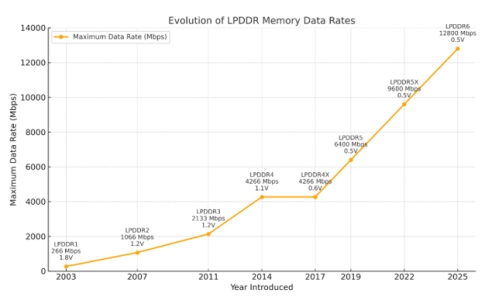
Figure 1: LPDDR Evolution and Standards
Power Efficiency
Energy efficiency is critical in both Electric Vehicles (EVs) and AI processors, which must deliver high performance under strict power constraints. AI workloads, ranging from deep learning inference to real-time analytics, demand substantial computing power. However, excessive energy use increases heat, cooling costs, and system inefficiency. Memory solutions like LPDDR5X, with Dynamic Voltage Scaling (DVS) and ultra-low operating voltages (down to 0.5V), help address these challenges by reducing heat and improving performance per watt, enabling faster and cooler AI processing at lower cost.
In EVs, every saved watt extends battery life and driving range, making efficient power management essential. High-speed, low-power memory like LPDDR5X is key to supporting advanced features such as ADAS, infotainment, and autonomous driving, delivering the required performance while conserving energy.
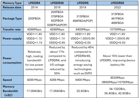
Table 1: LPDDR versions compared
Robust Reliability
In automotive, industrial, and AI applications, reliability is critical, where even minor data errors can lead to serious consequences. LPDDR5X incorporates advanced features to ensure consistent, high-speed performance in challenging environments:
- In-Line ECC corrects single-bit errors in real time, protecting data integrity in AI inference, ADAS, and automation systems.
- Decision Feedback Equalizers (DFE) reduce inter-symbol interference for clean, reliable signaling in noisy conditions like EVs and edge AI devices.
These capabilities make LPDDR5X a dependable choice for mission-critical, error-sensitive applications.
Advanced Bank Organization
LPDDR5X features an enhanced architecture with up to 16 banks and burst lengths of 16 or 32, enabling efficient handling of multiple data streams. Its multi-bank group mode reduces latency and boosts throughput.
This architecture accelerates AI model training and inference, while in ADAS, it ensures real-time sensor fusion by enabling fast, reliable data access and processing.
VT-Drift Compensation
LPDDR5X DRAM timing parameters can shift due to voltage and temperature drift over time, especially beyond 8533 Mbps in multi-rank scenarios. To maintain a reliable operational margin during the shrinking UI window under heavy loading, a sophisticated training scheme is often necessary from time to time, which was often not important in LPDDR4X applications.
Multi-Channel Configurations
Supporting x16, x32, and x64 data width configurations, LPDDR5X offers adaptability across different applications.
- Most mobile phones leverage x64 configuration with PoP (Package on Package) package for a small package size.
- AI inference processors optimize power and performance with x32 configurations with multiple memory devices.
- LPDDR5X offers multi-ranks and multi-dies in one package, making it a flexible choice for applications requiring large capacity or high speed.
3- LPDDR5X Key Design Challenges and Solutions
SI&PI simulation on the Package and PCB
LPDDR5X operates at up to 5.35GHz in single-ended transmission, causing crosstalk and reflection in the silicon substrate and PCB. More Signal Integrity analysis is necessary for planning the bump fanout in a small region and adding GND shielding to decrease the Crosstalk between high-speed signals.
A dual-rank LPDDR5X device will induce larger loading and worsen the reflection, which will decrease the EYE margin and cause obvious SI problems.
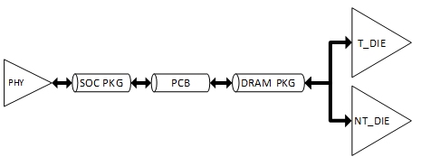
Figure 2: Topology of a double rank LPDDR5X device
Choosing optimized DRV/ODT parameters and adding equalization will significantly improve performance.
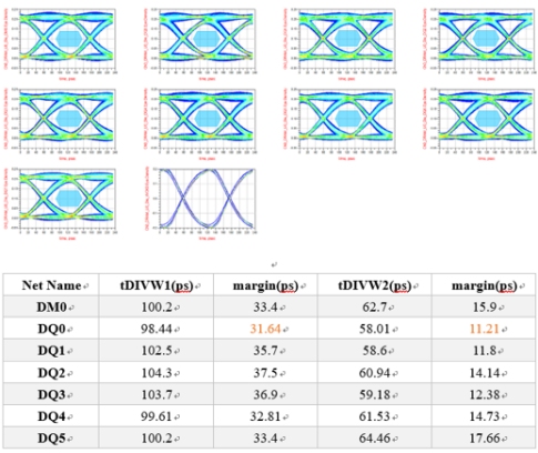
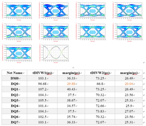
Figure 3: DQ eyes without and with equalizer
LPDDR5X operates at a lower IO voltage (0.5V), compared to previous generations, and therefore has a stricter power ripple requirement in power distribution design.
There are some methods to get the best power performance.
- Optimize the power nets path and get the lowest inductance at the package bumps
- Add the capacitors in the package and get the best optimization
- Adding more on-die Decap in metal layers
DFE for Enhanced Signal Integrity in LPDDR5X PHY
At ultra-high speeds (6.4–10.7 Gbps), maintaining signal integrity is critical. In LPDDR5X PHY IP, Decision Feedback Equalizer (DFE) is a key technology that combats inter-symbol interference (ISI) to sharpen the eye diagram and improve data reliability.
DFE works by combining a Feedforward Equalizer (FFE), which calculates the amount of interference for subsequent symbols based on the history of recent symbols.
Along with a multi-tap feedback loop that dynamically cancels ISI, based on previously received bits. Using adaptive algorithms, such as LMS (Least Mean Squares), the tap coefficients are continuously optimized to align with real-time channel conditions.
Designing an efficient DFE involves solving the following challenges:
- Timing Precision: Feedback and correction must occur within one UI (~93.1ps at 10.7Gbps), demanding ultra-fast logic paths.
- Power & Area Efficiency: Multi-tap DFE enables better ISI cancellation and better timing margin, but needs more area and power, and is a tradeoff designers should consider.
- Nonlinear Compensation: Crosstalk and reflections demand advanced modeling, sometimes using Volterra series-based techniques.
Despite these challenges, a DFE can boost eye height by up to 10%, enabling better timing margin and higher reliability.
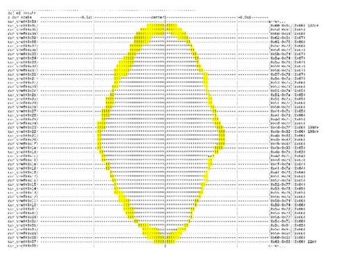
Figure 4: Variation of LPDDR5X RX Sampling Window with VT (The yellow region is the newly open eye after enabling the RX DFE function).
Optimization of Power Consumption and Performance through DVFS in PHY
Dynamic Voltage and Frequency Scaling (DVFS) is a powerful real-time power management technique that intelligently adjusts processor voltage and frequency to strike an optimal balance between energy efficiency and computational performance. It is a cornerstone of modern low-power design strategies, particularly effective in power-sensitive applications like mobile devices, EVs, and data centers.
In practical deployments across diverse customer use cases, DVFS has demonstrated up to 40% power reduction in GPUs under memory-intensive loads, 20–30% battery life extension in mobile devices, and 10–15% reductions in data center cooling costs—all while maintaining seamless performance scaling.
However, the benefits of DVFS come with significant design complexities that must be carefully managed to realize its full potential:
1- Timing convergence: When performing IP timing signoff, customers often demand support for a wide range of voltage and frequency combinations tailored to specific use cases. This necessitates multi-mode, multi-corner (MMMC) signoff, significantly increasing the complexity and cost of iterative timing closure. As the number of supported DVFS points grows, so does the validation matrix. In many cases, it becomes necessary to introduce design-level modifications to meet timing across all required operating conditions. Addressing this challenge demands close collaboration between skilled front-end and back-end teams, capable of navigating this design space and delivering customized, timing-robust IP optimized for real-world DVFS deployment.
2- Transient Response: This is another critical challenge in DVFS implementation. Since frequency and voltage transitions must occur simultaneously, these adjustments inevitably introduce latency, temporarily stalling upper-layer traffic. To mitigate this, system architects often resort to deploying large caches to buffer the stalled data flow. However, this workaround increases system complexity, adds area and power overhead, and may require significant architectural reconfiguration.
The impact of these delays can be minimized when the DDR PHY and controller IPs are designed with deep customization capabilities, allowing tight integration with the upper-layer SoCs. Several strategies can be employed to reduce latency and ensure smoother transitions:
- Implement hardware-accelerated frequency switching, embedding the frequency-cutting logic directly in hardware to enable rapid, deterministic transitions.
- Collaborate with the SoC to define voltage ramp profiles, including speed and mode (sequential or coupled) for VDD and VDDQ, ensuring the PHY has adequate margin for fast training during voltage changes.
- Leverage PLL lock period by enabling parallel operations, overlapping DFS events to reduce overall transition delays.
- Design the PHY architecture to support flexible frequency and voltage adaptation using multiple PLLs, thereby minimizing the overhead of voltage-frequency switching.
- Incorporate adaptable, multi-mode PHY training schemes that align with various DVFS scenarios, ensuring robust operation across dynamic conditions.
3- Link training: Link Training plays a critical role in enabling seamless DVFS transitions in the DDR PHY IP. During changes in operating frequency and voltage, the PHY is required to perform pre-training at each supported frequency to allow rapid switching. In parallel, real-time retraining is essential during voltage adjustments to compensate for variations in signal timing windows introduced by the change in supply levels. Variation in training requirements across different LPDDR5/5X/4/4X SDRAM cell types and manufacturers introduces significant design complexity. To ensure stable and reliable operation, especially in systems targeting broad DRAM compatibility, the PHY must be architected to handle a range of initialization and training behaviors.
A robust and production-ready LPDDR5X PHY IP is expected to address the following key challenges in the context of link training under DVFS:
- Training patterns must support multi-vendor compatibility, accommodating a wide variety of initialization sequences and DRAM cell behaviors.
- Flexibility in training modes is essential, with support for multiple pattern types, including enhanced PRBS, which is required to adapt to different operating conditions and DRAM requirements.
- Training strategies must balance robustness with time efficiency, minimizing performance impact while ensuring link stability.
- Optimization for timing and compatibility across DRAM vendors is necessary to deliver predictable and consistent performance across diverse system configurations.
To support dynamic scaling without disrupting data integrity, the LPDDR subsystem should be capable of autonomously selecting the appropriate training mode in response to DVFS events.
VT (Voltage & Temperature) Drift Compensation in PHY
The sensitivity of the data sampling window in the write direction and the alignment of read data with the clock can vary significantly across different LPDDR5X/5/4X/4 memory cells due to voltage, and temperature VT variations. During runtime, as temperature and voltage drift, the sampling window, particularly in the RX path, can shift, sometimes to positions that compromise timing margins and system stability.
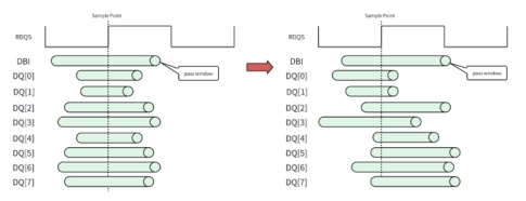
Figure 5: Variation of LPDDR5X RX Sampling Window with VT
For LPDDR5X/5, the presence of the On-die Sense Circuit (OSC) enables the system to periodically read mode register values and using vendor-provided mapping algorithms, determine the required compensation. The PHY can then dynamically adjust the delay lines for both read and write paths to maintain proper timing. This mechanism is validated through:
- Accurate characterization of delay vs. voltage/temperature across DRAM vendors
- Verification of OSC algorithm accuracy and timing closure at high speeds
- High-traffic stress testing to ensure no data integrity loss during real-time compensation
LPDDR5X/5/4X/4 relies on the PHY and controller to detect VT drift and adjust through internal training. Earlier implementations often struggled with inconsistent behavior across vendors, temperature cycling failures, and long training times, compounded by complex configuration requirements for different corner cases. A well-architected LPDDR PHY IP must address these challenges with:
- Reliable, vendor-neutral VT compensation training
- Backward-compatible methods for legacy DRAMs
- Reduced training time
- Simple, automated one-click compensation workflows
An effective VT compensation strategy is critical for ensuring robust DDR performance across varying environmental conditions and simplifying mass production deployment.
Performance Optimization of the Controller
The formula for calculating the system bandwidth for the entire DDR is as follows.
![]()
Optimizing the bandwidth of DDR controllers is a systematic and multi-dimensional process. The chart below (Figure 10) illustrates the performance curve observed during the optimization process. This curve helps track performance trends and provides detailed performance data.
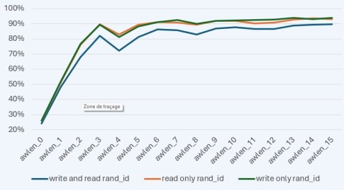
Figure 6: Bandwidth Optimized Result example
At the system level, optimization includes command pre-scheduling via memory schedulers and effective address interleaving. Internally, the DDR controller applies several advanced techniques to enhance efficiency and maximize throughput:
- Interface-level command distribution to ensure high-priority commands are not blocked by lower-priority ones.
- Read data reordering to resolve protocol-level issues caused by out-of-order command execution during optimization.
- Multi-port arbitration policies to balance read/write switching and ensure high-priority commands are efficiently scheduled.
- Address conflict resolution for read/write operations to improve consistency and reduce delays from blocked SoC-level commands.
- Write command consolidation to reduce operations involving write masks and eliminate redundant commands.
- Dynamic read/write direction switching to minimize timing delays such as tWTR, tRTW, and tRCD.
- Kernel-level scheduling to prioritize urgent or high-priority commands under bandwidth pressure.
- Command prioritization strategies that ensure time-sensitive commands are given precedence across different scenarios.
- Row activation/deactivation policies to reduce precharge-to-active delays and adapt to varying SoC access patterns.
- Adaptive auto-refresh mechanisms to minimize performance impact during self-refresh cycles.
- Flexible address mapping policies to reduce row conflicts and hidden bank activations, aligned with SoC traffic behavior.
In addition to these architectural strategies, IP vendors must provide robust analysis tools to evaluate controller performance. These tools are essential for measuring latency and bandwidth under specific traffic scenarios. For instance, the figure below shows an AXI Access Latency Bar Chart, which visualizes all AXI transactions across different latency ranges, helping designers track and debug access performance more effectively.
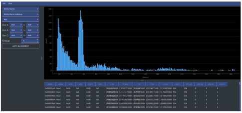
Figure 7: Performance Optimized Tool
4- Innosilicon LPDDR5X/5/4X/4 Combo IP Subsystem
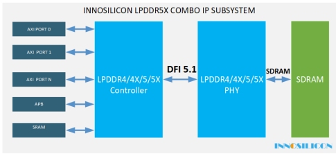
Figure 8: Innosilicon LPDDR5X Combo Subsystem Solution
Innosilicon’s LPDDR5X/5 Combo IP Subsystem (PHY + Controller) delivers up to 42.8 GB/s of bandwidth (x32, 10.7 Gbps per DQ), enabling real-time data processing for all modern-day applications. The latest LPDDR5X generation enhances performance with a 17% increase in transmission rate and a 15% reduction in transmission delays. This technology has been rigorously validated and silicon-proven at all advanced process nodes from 14/12nm all the way down to 3nm, ensuring seamless scalability and reliability.
A key milestone in LPDDR5X development is Innosilicon’s 10.7 Gbps transmission on standard PCB boards, demonstrating industry leadership in memory interface technology.
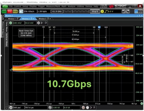
Figure 9: 10.7 Gbps Eye Diagram Measured on PCB board
Designed for both PCB and substrate level transmission, Innosilicon’s LPDDR5X IP offers:
- Complete LPDDR5X/5/4/4X combo controller and PHY solutions for total performance optimization under multi-rank scenarios.
- Innosilicon provides LPDDR5X IP in both 32-bit and 64-bit configurations, catering to diverse system design and bandwidth demands.
- Sophisticated training schemes to maintain higher signal margins ensure reliable high-speed data transfers.
- Integration of Dynamic Voltage and Frequency Scaling (DVFS) and low-power modes such as Deep Sleep and Hold minimizes power consumption during idle periods and allows for deep customization in conjunction with customers.
- By reducing silicon area by 20 to 30 percent, Innosilicon Combo IP simplifies integration in space-constrained designs. Its compact package size enhances thermal management capabilities and reduces PCB manufacturing costs, optimizing performance for high-performance, low-power applications.
- Integrated RX DFE feature significantly increases eye height and ensures perfect eye diagrams at 10.7 Gbps.
- Automatic retraining mechanism enables the memory subsystem to self-tune to temperature changes and voltage variations, ensuring long-term stability without interrupting operation.
- Full-flow hardware auto-training process and DFX diagnostic tool to complete the adaptation and mass production testing of all LPDDR series cells available for sale.
- Innosilicon’s LPDDR5X/5/4X/4 has powered mass production for several customers across FinFET nodes since 2018, spanning autonomous driving, AI, and consumer electronics. With standard delivery, one-click firmware generation tool, complete test support, and deep customization, it accelerates integration and helps customers achieve faster time-to-market success.
- Fully compliant with stringent vehicle standards such as ISO26262, AEC-Q100, ensuring reliability in mission-critical Automotive applications.
On-Die Scope
The On-Die Scope (ODS) feature in Innosilicon’s LPDDR5X is an embedded debugging and monitoring tool that provides real-time visibility into internal memory operations.
By capturing critical signal activity without requiring external probing, ODS enables efficient debugging, performance optimization, and system-level validation. It allows engineers to analyze timing, power consumption, and signal integrity issues, ensuring reliable operation in high-speed applications. Additionally, by eliminating the need for expensive external test equipment and complex probing setups, ODS significantly reduces validation costs while streamlining the development process. This integrated diagnostic capability simplifies debugging, minimizes design iterations, and enhances overall memory performance and reliability.
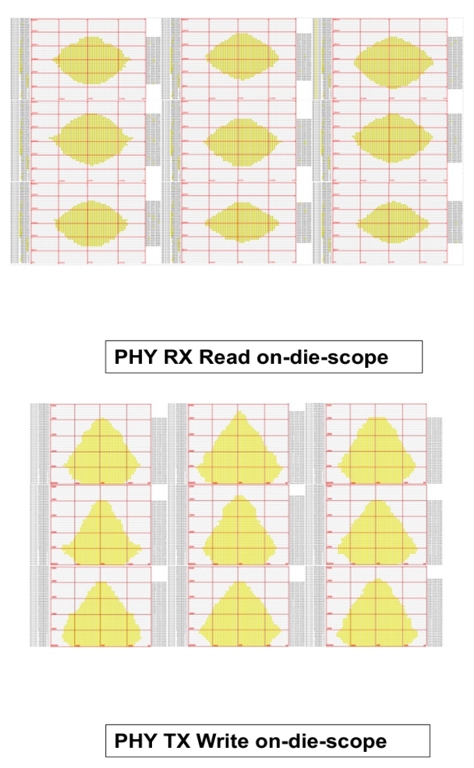
Figure 10: Verifying the Eye Diagrams using ODS on Innosilicon LPDDR5X Combo IP
Innosilicon is positioned to lead the next phase of memory innovation with LPDDR6, expecting to achieve data rates of up to 14.4 Gbps. Through strategic partnerships with all major memory vendors and continuous R&D, the company remains at the forefront of DDR advancements, delivering cutting-edge solutions for future computing demands.
Summary
LPDDR5X is at the forefront of modern memory solutions, enabling high-performance applications across AI, Mobile Computing, IoT, and Automotive systems. With its combination of high bandwidth, low latency, high capacity, power efficiency, and robust reliability, LPDDR5X serves as the ideal memory technology for industries pushing the boundaries of performance and innovation.
Innosilicon’s LPDDR5X/5/4X/4 Combo IP further enhances these capabilities, delivering a silicon-proven, mass-produced solution, tailored for highest-speed, energy-efficient applications. As technology advances, LPDDR5X stands as the foundation for next-generation computing, driving forward smart, efficient, and AI-driven ecosystems.
About Innosilicon
Innosilicon is a leading global provider of High-Speed IP and ASIC design services, enabling customers to shorten time-to-market, reduce risk and design cost.
Founded in 2006, the company has established itself as a reliable IP provider and well-recognized in the semiconductor industry. Innosilicon supported over 300 top-tier clients, enabling them to increase their time-to-market and limit design risk, shipping more than 10 billion high-end SoCs and developing silicon solutions in FinFet processes across all major foundries. Innosilicon is committed to driving global innovation by leveraging its extensive chip design expertise and deep partnerships with semiconductor foundries, like TSMC, Samsung, Global Foundries and others, striving toward customer success.
Innosilicon stands at the forefront of memory interface innovation, redefining what’s possible in high-speed DDR and LPDDR technology. As the first in the industry to push GDDR6 to 24 Gbps using NRZ signaling, Innosilicon has proven its ability to break barriers where other IP vendors follow. This same cutting-edge IP has been expertly scaled down to drive LPDDR5X performance up to 10.7 Gbps, bringing unprecedented reliability and speed to mobile and AI memory applications. With full-stack mastery of high-speed I/O, Innosilicon delivers not only world-class PHYs but also highly customizable controllers, tailored to the unique needs of workloads like large language models, where read efficiency is paramount. Whether it’s a bandwidth-hungry AI, next-gen mobile, or edge compute, Innosilicon’s memory solutions are built to stay ahead, fast, flexible, and future-ready. During the last
two decades, the company has worked on applications, such as high-performance computing, Multimedia, Automotive, AI, and IoT applications, and developed an extensive IP portfolio ranging from HBM3E/4, GDDR7/6X/6, UCIe Chiplet, PCIe6/5/4, among others.

Figure 11 Innosilicon's IP Offering
Innosilicon Technology Inc.
97 E Brokaw Rd #210,
San Jose, CA 95112
For more information, contact sales@innosilicon.com