by David Schwaderer, Philippe Martin, Sonics Inc.
Mt. View, California (USA)
Introduction
Following the invention of the transistor in 1947, advanced circuit designers soon discovered that their discrete component designs required many unreliable, hand-soldered connections. This rendered these components increasingly difficult, if not impossible, to manufacture. The intractable problem became known as the tyrrany of numbers or interconnections problem[1].
While the integrated circuit subsequently provided the physical ability to manufacture the advanced electronic circuits engineers could logically design, its continued density progression following Moore’s Law has introduced a converse interconnections problem. Although increasing sub-micron densities now enable the physical manufacture of virtually any circuit, the resulting massive increase in size (gate count) and complexity has made it increasingly difficult, and sometimes impossible to design advanced circuit logic economically and reliably within competitive schedules.
The MicroNetwork – an on-chip communications structure that provides a fast, highly efficient, application-specific, on-chip communications network – has proven effective in alleviating the interconnections problem encountered with today’s system-on-chip (SOC) designs. However, the same pressures that have driven the SOC revolution, i.e., shrinking area, cost, and power requirements, now has engineers searching for a way to fulfill all of the shared memory requirements posed by an SOC’s various initiators (such as processors, DMA engines, and specialized hardware cores) with a single DRAM subsystem. This paper will address the conundrum SOC designers now face: how does one achieve both high DRAM utilization and guaranteed quality-of-service (QoS) when multiple, disparate data flows share a DRAM subsystem?
Problem Statement
Increasingly powerful SOC designs require ever-larger memories. Usually, these memories comprise a single shared memory. For design economy reasons and limited external pin availability, these memories are often external to the SOC.
The efficiency with which the system handles non-deterministic shared-memory accesses is paramount. However, introducing global access optimizations can prevent the system from fulfilling the strict service-level requirements for individual initiators. Thus, providing efficient shared memory utilization and meeting specified service-level guarantees are conflicting design goals that require individual optimization control. Consequently, shared memory performance problems are often the most frequent and difficult performance problems SOC designers encounter.
Consider that a single memory reference exhibits a latency consisting of two components. The first component (S) consists of clock cycles required for fulfillment setup delays. These include RAS and CAS cycles, a possible page close delay to restore bit values following a destructive read, DRAM bus turn-around delays occurring from alternating read and write operations, etc. The second category consists of the number of clock cycles required to effect the actual read or write transfer following the setup delay.
In a two-transfer burst, each transfer requiring one cycle, total time for the burst would be S+2T, for an N-transfer burst, the total clock cycles required for a burst is S+NT (assuming the burst sequence requires only one setup activity). For increasing values of N, bursts clearly become increasingly efficient from a memory bandwidth transfer metric since they amortize the initial setup delay over a large number of subsequent transfers. Consequently, DRAM designs consider these two categories and have evolved various strategies to offset the effects of the first category. The most common are page mode and bank switching operational modes.

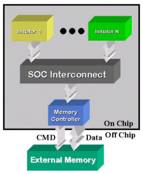
Figure 1 - An SOC interconnect that supplies only one communication channel per IP core and interleaves bursts presents a single memory reference request stream to a shared memory controller. The interleaved stream will exhibit diffused memory reference locality.
The reality for SOCs is that N usually equals one. From Figure 1, consider that an SOC usually com-prises a number of initiator cores that present requests to memory. Over time, an individual processing activity within one such core generates a memory reference stream (reads and writes). Usually, these collective references exhibit temporal and spatial locality. However, note that a single processor often simultaneously presents three such memory reference streams to memory. These are associated with:
1. Instruction fetching
2. Stack operations
3. Data inspection and manipulation
Since SOC designs usually incorporate multiple initiators, each having differing bandwidth and latency requirements, it is easy to understand why memory access is usually the SOC performance bottleneck and so difficult to achieve within service-level guarantees:
- DRAM designs are optimized to fulfill long sequential bursts and less suited to handle random memory reference operations;
- A single initiator generates multiple memory reference streams with different reference locality characteristics;
- SOC designs incorporate increasing numbers of initiators that have varying QoS requirements and latency sensitivities;
- Effective SOC designs use transport mechanisms that enables fine-grained interleaving;
- Interrupting an in-progress burst request to service another incurs a set-up penalty, but this may be necessary to meet guaranteed service times;
- When collective memory references converge on a single external DRAM memory controller as a unified request stream, the consequent request stream exhibits no coherence, hence is essentially indistinguishable from a randomly generated request stream.
Thus, SOC designs naturally diffuse shared initiator memory reference localities, placing at risk the SOC’s performance requirements. Most of today’s design approaches usually demand notable engineering skill to get the system operational (extending development schedules). These approaches usually involve multiple conventional buses or special purpose busses from initiators to some sort of arbitrator near the memory controller[2,3]. However these incremental approaches do not scale, and present cross talk, timing convergence problems, and general congestion challenges while precluding genuine core reusability [4]. These ad-hoc approaches mimic the well-intended but eventually futile attempts by cargo sailing ship designers to exceed steam ship efficiencies by adding additional masts to their ship’s designs.
Sonics’ design engineers have encountered numerous examples of this design approach while reviewing proposed customer designs, many requiring on the order of 6,000 converging wires. These signal wires would individually experience poor utilization despite their endemic die area and power expense. To exacerbate matters, the resulting erratic, non-deterministic memory subsystem performance generally requires initiator cores to utilize significant buffer storage in an effort to isolate processing from non-deterministic memory latencies[6].
Historically, SOC system designers have faced these shared memory contention challenges with inadequate tools and methodology to proceed systematically and efficiently. However, recent intelligent memory access scheduler designs and modeling tools, combined with commercially available MicroNetwork solutions, now offer critical assistance in maximizing shared memory access efficiency. This activity is particularly challenging since, as previously stated, increasing transfer bandwidth and decreasing response latencies are conflicting goals.
Solution Overview
SOC memory sharing presents several challenges:
- Physical interconnection to a shared memory
- Concurrent multiprocessor shared memory access
- Service-level guarantees
- System performance
This paper proposes a design methodology that utilizes the following elements to address all these challenges:
- The Open Core Protocol (OCP)
- The SiliconBackplaneâ„¢ MicroNetwork
- The MemMaxâ„¢ Memory Access Scheduler
- The Sonics Graphical SOC Design, Modeling, and Test Tools
These elements collectively provide designers with the essential architectural features and shared memory operational visibility necessary to design systems exhibiting optimized system performance. The key architectural methodology borrows from Local Area Network (LAN) concepts that provide high-performance communication between heterogeneous entities via a translucent shared transport mechanism. These architectural approaches are directly applicable to SOC designs and provide similar implementation flexibility.
The Open Core Protocol (OCP)
The concept of a rapid-time-to-market SOC is inseparable from the requirement for independently created, reusable semiconductor intellectual-property (IP) cores[5]. OCP is an internationally supported IP core interconnection standard advanced by the OCP International Partnership, or OCP-IP (www.opcip.org). OCP provides cores with significant modularity that increases genuine design reusability without core rework.
OCP provides a combined communication protocol and hardware connection scheme for SOC logic blocks. As a protocol, OCP provides a minimal command set for memory-mapped, split-transaction activities such as read, write, and read exclusive. (Read exclusive is a command variant of the read command specifically designed for use within semaphore processing.) These atomic activities occur over threads – communication channels that guarantee the response sequence order matches that of the original associated requests. Thread tags accompanying memory-mapped requests therefore providing an efficient way to present requests from an OCP master interface to an OCP slave interface.
Slaves can independently process requests arriving on different threads using any priority algorithm or use the thread tags to vector the individual requests to different independent logic such as different DRAM banks[9]. However, on any single thread, a slave core must preserve the response order, though there is no consideration for order preservation across collective threads. This consideration is essential when the slave core is a DRAM memory controller. Here, in-order responses guarantee a stringent memory consistency model generally required for coherent multiprocessor system operation.
Finally, OCP has a number of extensions in addition to threads. One key extension is burst support, which provides slave cores hints that might enable them to optimize operations. For more OCP information and how it supports control and test signals see the Open Core Protocol Specification available from www.ocpip.org.
In summary, OCP is a standard socket architecture that provides a configurable socket interface and simple protocol for IP cores. Simplicity is essential because “All freshly designed protocols, no matter how disciplined their designers have been, must be treated with suspicion. Every protocol should be considered to be incorrect until the opposite is proven.â€[7]

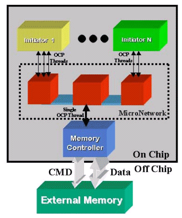
Figure 2 - An OCP-based SOC MicroNetwork can supply multiple communication channels per IP core. However, a typical memory controller can only use one communication channel, so all communication channel traffic must arrive on one channel. Hence, the aggregate memory reference locality still diffuses.
The SiliconBackplane MicroNetwork
The SiliconBackplane is an intermediary SOC interconnect for IP cores designed with OCP interfaces (Figure 2). IP cores, called initiators, launch work requests through their master OCP socket interface. The SiliconBackplane preserves associated request thread information and assists burst efficiency by insuring that recipient threads receive uninterrupted burst requests. Also, SiliconBackplane multiplexing guarantees bandwidth service-levels to cores while simultaneously reclaiming assigned, but unused bandwidth. An SOC SiliconBackplane complex shares a single, maximum 32-bit address space. Assigned memory space ranges enable targets to determine when work requests are directed at them.
The SiliconBackplane enables fine-grained traffic burst interleaving, unlike traditional bus architectures. In the networking world, the SiliconBackplane approximates the transmission granularities and prioritized latency considerations of cell-switching technologies such as asynchronous transfer mode (ATM), without sacrificing the efficiency advantages of sustained bursts. Finally, bandwidth allocations, target address ranges as well as many other SiliconBackplane parameters are completely reprogrammable by initiator cores when workload and traffic patterns dynamically change.
The MemMax Memory Scheduler
SiliconBackplane solves wiring convergence problems by providing a compact, high-bandwidth OCP connection for IP core attachments including memory controllers. This isolates the DRAM efficiency maximization challenge to the memory subsystem. However, the challenge cannot be addressed independently from guaranteed service-level requirements.

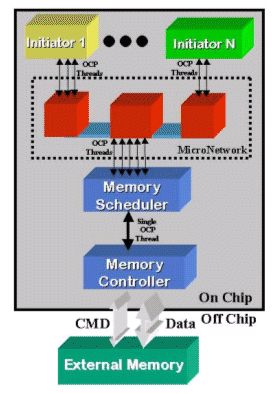
Figure 3 - A memory scheduler connects to an OCP-based MicroNetwork using multiple communications channels and to a traditional memory controller that only uses one channel.
Referencing Figure 3, DRAM controllers traditionally receive memory requests over a single command (CMD) channel. If the CMD channel is an OCP interface that connects to a SiliconBackplane, this single OCP interface receives entire bursts due to the SiliconBackplane burst efficiency considerations. In practice, the DRAM efficiency requirement can be resolved by inserting intermediary multi-threaded logic between the SiliconBackplane and the memory controller. Optimally, this logic would exploit its ability to receive multiple, unrelated, interleaved bursts to reestablish memory referential locality within service-level requirements. This logic exists and is called the MemMax Memory Scheduler[6].
MemMax is a configurable IP core that balances the conflicting goals of increasing memory efficiency while maintaining service-level guarantees for dependent initiator cores. MemMax comprises:
- A multi-threaded OCP interface that attaches to the SiliconBackplane MicroNetwork – having multiple threads allows multiple in-flight bursts that the SiliconBackplane transports in a fine-grained manner;
- Logic that temporally reorders pending head-of-queue requests from different threads to maximize DRAM efficiency – this enables MemMax to construct request sequences that mimic bursts but are from different threads;
- A single-thread OCP interface that passes a sequential request stream to a standard DRAM controller with an OCP interface.
With MemMax, subsystem configuration is a two-step process. An initiator first configures the DRAM controller through the MemMax scheduler to establish memory controller operating modes (bank switching, auto-precharge/page mode, etc.). Then, the MemMax scheduler is configured to observe service-level requirements. Subsequent MemMax operations then present memory requests that are maximally efficient within these constraints.
In operation, an individual request is presented to the memory controller when it wins a filtration contest (Figure 4). In this way, MemMax re-imposes a measure of locality over a multiplicity of unrelated request streams that incorporates DRAM configuration and design considerations (page or bank switching mode, auto-precharge support, etc.). Modeling indicates that MemMax can improve performance by as much as 42 percent[6]. Finally, MemMax achieves DRAM technology independence by exploiting conventional DRAM controllers that interface to external DRAM memory whose performance levels are continuously evolving.

Figure 4 - A multi-communication-channel filter stack within a memory scheduler intervening between a multi-channel MicroNetwork and memory controller can transparently help intermix and present unrelated memory request streams in a way that re-establishes memory reference locality. This maximizes SOC memory reference efficiency, resulting in lower memory power consumption through decreased operating frequency. However this interleaving must honor service-level guarantees.
The Sonics Development Environment
The Sonics Development Environment comprises two development programs – CoreCreator and SOCCreator. CoreCreator enables IP core designers to test individual IP core OCP interfaces and core designs in isolation from other SOC components. It accomplishes this by augmenting existing tools with master and slave OCP behavioral models that interact with respective counterpart core designs during CoreCreator simulations. CoreCreator provides a modeling language called Socket Transaction Language (STL) that enables designers to verify OCP slave interface correctness as well as in-test OCP slave core functionality. Post-processing programs process simulation logs to produce a variety of core OCP performance reports.
SOCCreator enables SOC designers to integrate and test IP core and SiliconBackplane SOC designs. It also enables designers to utilize CoreCreator STL test benches to verify end-to-end system connectivity behaviors, thereby delivering a portable test bench. However, designers must still verify correctness of shared memory interactions between initiators such as semaphore utilization. Finally, SOCCreator also enables SOC simulations incorporating native core stimulus and existing simulation tools.
By allowing SOC simulations to temporarily substitute behavioral models in place of yet-undeveloped cores, SOC architects can identify shared memory performance bottlenecks in the first few hours of a development effort, enabling IP core design, preliminary layout, and system performance testing to overlap – giving earliest views of system behaviors that could prove problematic. Lastly, both CoreCreator and SOCCreator provide an intuitive graphical user interface that designers can use in lieu of an optional command line interface.
Conclusion
Solving SOC Shared Memory Challenges is not an incremental fix. It is a design methodology that begins with atomic split-transaction operations that support multiprocessing and exploits multi-threaded MicroNetwork interconnections and opportunistic external memory access optimizations. The design process proceeds under appropriate test and design environments that exploit existing designers’ tools and skill sets. Hence, solving SOC shared memory challenges is an outcome of methodology philosophy. The salient point is that just as a new mind set was required to solve the interconnections problem in 1958, so it is with today’s SOC designs.
The SiliconBackplane MicroNetwork is now successfully deployed. MemMax is now being incorporated into commercial designs that are about to enter production. Like the integrated circuit was to discrete component designs, OCP, the SiliconBack-plane MicroNetwork, MemMax, and the Sonics development environment represent a new develop-ment paradigm. Their existence opens opportunities for unprecedented rapid time-to-market development. However, in balance, as Max Planck suggested:
An important scientific innovation rarely makes its way by gradually winning over and converting its opponents… What does happen is that its opponents gradually die out and that the growing generation is familiarized with the idea from the beginning: another instance of the fact that the future lies with youth.[8]
MicroNetwork-based methodology adopters can therefore expect to compete against development teams who cherish their traditional development methodologies. The crew of the Thomas W. Lawson received a first-hand experience of the inevitable outcome of incremental extensions to traditional approaches.
Succinctly then, those who cannot remember the past are condemned to repeat it (George Santayana, Reason in Common Sense). The bright note is that skillful engineers within traditional methodology design teams will easily reincarnate within the agile design groups that elect to adopt MicroNetwork design methodologies. As is quipped in Grenoble, “Bonne chance mes amis!â€
[1] T. Reid, “The Chip: How Two Americans Invented the Microchip and Launched a Revolutionâ€, Random House; ISBN: 0375758283; October 9, 2001[2] L. Benini and G. De Micheli, “Networks on chips: A New SoC Paradigmâ€, IEEE Computer, January 2002
[3] L. Benini and G. De Micheli, “Networks on chips: A New System on Chip Paradigmâ€, International Conference on Design and Test Europe, 2002
[4] K. Goossens et al., “Networks on Silicon: Combining Best Effort and Guaranteed Servicesâ€, International Conference on Design and Test Europe, 2002
[5] D. Wingard, “On-chip networks: the secret to high-performance communication SoCs, flexible platformsâ€, Integrated Communications Design, August 2000
[6] W. Weber, “Efficient Shared DRAM Subsystems for SOCsâ€, Microprocessor Forum, 2001
[7] G. Holzmann, Design and Validation of Computer Protocols, Prentice Hall, 1990
[8] M. Planck, Philosophy of Physics, 1936 German Translation
[9] D. Wingard et al., "Smarter Interconnects for Smarter Chips", presented at Hot Chips, 14 August, 2002
1 The last implementation of this specific incremental algorithm was by Bowdoin B. Crowninshield, the designer of the Thomas W. Lawson, a steel cargo schooner constructed with seven massive masts. It was so top heavy, it capsized at anchor in a severe gale, killing everyone aboard except the captain and one other ship hand.
