
3D heterogeneous integration (3DHI) technology creates high-performance systems by integrating different types of semiconductor chips or chiplets stacked vertically. Diverse functions such as processing, memory, and RF can thus be combined onto a single chip or package to improve performance and efficiency. As 3DHI systems increase in complexity, the importance of the Universal Chiplet Interconnect Express (UCIe) standard is becoming critical to the future of advanced packaging and semiconductor system design. The expertise for these technologies and the exponentially increasing computational demands are lengthening design times and increasing time to market.
A paper presented at the 2025 Government Microcircuit Applications & Critical Technology Conference (GoMACTech) explores the trends in the industry and highlights a Cadence solution that has been developed specifically to streamline the design flow by providing UCIe full signal integrity analysis with compliance check for heterogeneous integration. This paper details the analysis solution and design architecture with various test cases from Cadence and its customers who continually push the industry standards and challenge the existing analysis capabilities currently available.
Heterogeneous Integration
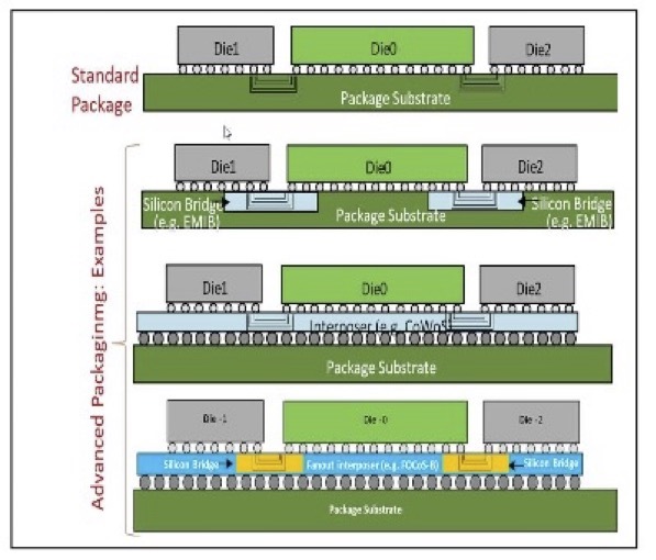
Heterogeneous integration is a trend many industry leaders are currently pioneering. Figure 1 shows standard and advanced packaging 2D and 3D scenarios.
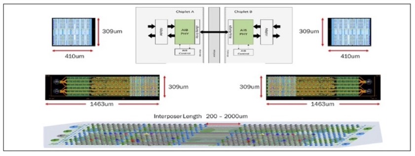
One prerequisite for the large-scale use of chiplets is the emergence of interconnect standards such as UCIe and robust tools and design flows that support the problems unique to chiplets. This paper discusses the heterogeneous integration of a silicon interposer that is optimized for 960Gbps data transfer using the UCIe interface. While the design and verification of the input/output ( I/O) and µbump array on the chiplets followed a standard IC development flow, the integration of the chiplets on the silicon interposer required a new design flow to completely model the signal impairments caused by the interposer. Figure 2 shows the key elements of the UCIe interface.
Full Signal Integrity Flow
Full simulation and analysis for signal and power integrity (SI/PI) is integral to system design (Figure 3).
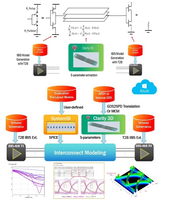
Cadence Sigrity Signal and Power Integrity and Clarity 3D Solver multiphysics systems analysis (MSA) software were utilized for the full simulation of the design. The transistor-to-behavioral (T2B) model conversion within the Sigrity SystemSI UCIe compliance kit and the Clarity 3D Layout tool provided UCIe full signal integrity analysis with compliance check for heterogeneous integration. T2B was used to generate the IBIS I/O buffer information specification model from the transistor-level Intrinsix IP design. SystemSI was used for the transient (time domain) analysis and automated UCIe compliance kit checking. Clarity 3D Layout was used for the full-wave 3D finite element method (FEM) S-parameter extraction of the UCIe interface routed on the interposer.
Conclusion
This GOMAC talk presents a detailed solution leveraging Cadence Sigrity/Clarity, Allegro, and Virtuoso platforms that comprises a complete flow, including a full 3D extraction for an 8-layer silicon interposer optimized for 960Gbps data transfer using the UCIe interface. The flow provides UCIe full signal integrity analysis with compliance check for heterogeneous integration that also allows detailed simulation of transmission line effects on the interposer. The full paper with technical details is available here.