
Chiplet-based, multi-die systems are gaining traction as a compelling alternative to monolithic system-on-chip (SoC) designs. These architectures are enabled by die-to-die (D2D) connectivity advances and driven by the need to overcome reticle limitations and improve yield. Designers can integrate homogeneous or heterogeneous functions, with each die implemented using the most appropriate process node for performance, power, and area. This disaggregation introduces new design challenges, including system-level integration, handling coherent and non-coherent traffic, and managing register address mapping across multiple dies.
There are several practical reasons for this momentum. One of the most important is that it allows engineers to create systems that exceed the physical limitations of a single monolithic die, which is 858 mm2 at the time of writing. By distributing functionality across multiple smaller dies, these architectures enable the implementation of larger, more capable designs within a single package.
Smaller individual dies also tend to yield better during manufacturing, which can lead to significant cost savings at scale. Beyond economics, chiplets introduce new flexibility into design strategy. Processing elements such as CPUs, GPUs, NPUs, and other accelerators can be selected for their strengths and combined with in-package memory or interface controllers to meet specific performance goals.
These systems may be composed of identical processing units that scale performance through replication or a mix of different elements that each serve a specialized role. For example, multi-die SoC designs can incorporate high-speed logic in 3 nm, dense SRAM in 7 nm, and high-voltage I/O on a 28 nm process. Teams can reuse existing components and more easily build product variations by reconfiguring the chiplet assembly rather than redesigning the entire system.
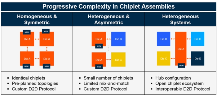
Figure 1 – Progressing complexity in chiplet assemblies (Source: Arteris, Inc.)
Building Chiplet Ecosystems
Today, many companies are developing multi-die systems. Some, like AMD, Intel, and Nvidia, manage the entire development process in-house. Due to deep pockets, these companies can create highly customized solutions tailored to their specific performance and integration goals.
By contrast, many larger companies and startups are exploring collaborative approaches. By working with trusted partners, these companies create ecosystems that combine specialized expertise across IP, packaging, and manufacturing. This model enables them to co-develop solutions while distributing risk and development costs more effectively. D2D interconnect standards like UCIe are often used as a partnership baseline. Proprietary extensions may be added to meet specific performance, coherency, or protocol requirements.
This transition to chiplet-based design has encouraged ecosystem partners to improve design flows and interoperability. Many EDA and IP vendors collaborate to develop standards, reference architectures, and automation tools that simplify integration across dies. The result is a more robust and maturing toolchain that supports custom and standardized chiplet-based development. As chiplet architectures become more modular and scalable, the industry is responding by developing the infrastructure and partnerships needed to support broader adoption.
Arteris Multi-Die Solution
Arteris has established itself as a leader in network-on-chip (NoC) IP interconnect technologies, offering silicon-proven solutions integral to chiplet-based SoC designs. Its portfolio includes the non-coherent FlexNoC and FlexGen interconnect IPs and the coherent Ncore interconnect IP. While traditional single-die SoCs rely on one or more NoCs to connect internal IP blocks, multi-die systems introduce a more distributed approach, where each chiplet can incorporate its own NoC. These chiplet-level interconnects are linked using high-bandwidth, low-latency bridges that support D2D communication, allowing the system to operate as a functionally monolithic design.
The company further simplifies the design of multi-die systems through automation. Its Magillem Connectivity and Magillem Registers products streamline validation and SoC integration and unify hardware and software views across the full system map. This enables faster assembly and documentation with reduced engineering overhead and risk.
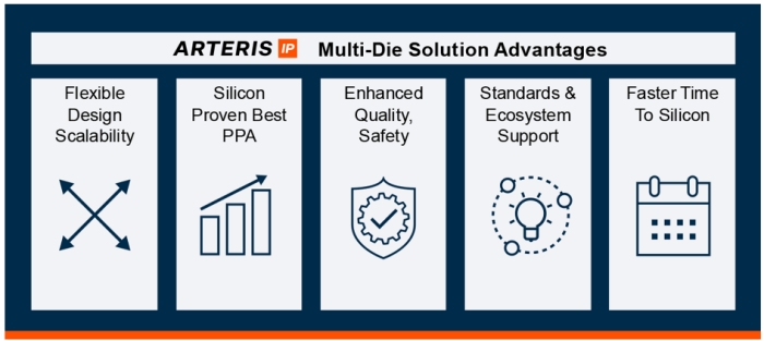
Figure 2 – Advantages of Arteris’ multi-die solution (Source: Arteris, Inc.)
The Arteris Multi-Die Solution includes:
- Silicon-proven non-coherent FlexNoC IP supports the relevant standards and integrates with third-party commercially available D2D controllers and PHYs.
- New cache-coherent Ncore NoC IP capabilities enabling seamless cache-coherent reads and writes across multiple chiplets, making multi-die systems look like a single piece of silicon to application software programmers.
- Magillem Connectivity automation for SoC assembly from IP and chiplets, reducing project risks associated with manual, error-prone integration tasks.
- Magillem Registers automation for integrating hardware and software from system map definition to validation and documentation based on a single source of truth.
The Arteris multi-die solution enables connectivity across chiplets, supporting coherent and non-coherent traffic and intelligent dataflow management. By supporting leading standards such as UCIe, Arm AMBA protocols, and PCIe, the Arteris solution fosters broad interoperability. Integration with PHY IP and D2D controllers ensures compatibility with commercial implementations. Support for tool flows from leading EDA vendors and foundries streamlines D2D silicon realization.
Conclusion
As the semiconductor industry moves toward broader adoption of multi-die architectures, success will depend not only on hardware innovation but also on managing efficient system integration. Solutions that unify hardware and software views while reducing manual effort are becoming essential to meet project schedules and complexity demands. Arteris addresses these needs with proven automation and integration capabilities that help design teams move from concept to silicon with greater confidence and speed.
About the author

Andy Nightingale, VP of product management and marketing at Arteris, has over 37 years of experience in the high-tech industry, including 23 years in various engineering and product management positions at Arm.