
In advanced process nodes, the severe decoupling between SRAM scaling stagnation and logic circuit scaling, combined with the surging on-chip memory demands from Large Language Model (LLM) training and large-scale inference applications, has made SRAM a critical factor determining yield and long-term reliability. Facing the yield cliff challenge, traditional eFuse technology has reached its physical limits and can no longer handle massive repair requirements. This solution proposed here is to combine eMemory’s high-capacity NeoFuse one-time programmable (OTP) memory with Siemens’ Tessent™ MemoryBIST Built-in Self Repair (BISR) capabilities, to enable an innovative two-phase repair with the ability to perform in-field incremental repair of SRAM. This solution not only significantly improves wafer yield by increasing the number of good dies per wafer during manufacturing but also enables chips to achieve self-healing capabilities throughout their entire lifecycle.
Scaling Issues & Yield Cliff Challenges of SRAM at Advanced Nodes
As semiconductor technology advances to the 3nm and 2nm nodes, the semiconductor industry faces increasing constraints by the dual pressure from device physics and application demand. While logic density continues to improve, high-density SRAM bitcell area has shown only modest reductions – plateauing at approximately 0.021 µm² at 3nm and shrinking to about 0.0175 µm² at 2nm. At the same time, generative AI training and inference workloads have driven a sharp increase in on-chip SRAM demand, causing SRAM to occupy 30–50% of die area in mainstream AI accelerators and up to 60–70% in SRAM-centric designs.
While row and column redundancy are standard features in SRAM design, the traditional storage capacity for repair signatures, typically limited to tens of kilobits, is becoming increasingly inadequate as the SRAM repair demand reaches gigabit levels at 3nm. Focusing solely on SRAM macros, when defect density approaches 0.5–1.0 defects/cm², the combined impact of random hard defects and Vmin-limited parametric failures rapidly exhausts available redundancy resources. Once the defect count surpasses the repair threshold, the SRAM post-repair yield suffers a precipitous drop – potentially plummeting to below 60%. This indicates that for large-area chips, physical redundancy alone is insufficient; the bottleneck in storage for repair data is emerging as a silent killer of advanced-node yield.
The Physical Limits of eFuse for AI SRAM Repair
eFuse, once the standard repair solution, faces fundamental barriers at advanced nodes.
- Serious challenges in back-end-of-line (BEOL) power routing. eFuse programming relies on metal electromigration and requires peak currents of ~100–150 mA delivered through extremely low-resistance paths that are typically <2 Ω. In modern AI SoCs with hundreds of megabytes to gigabytes of SRAM, such high-current routing places severe stress on an already congested BEOL metal stack, creating power integrity, routing, and floor planning challenges.
- Repair metadata reaches the megabit range. While raw SRAM bit defect rates remain on the order of ~1 ppm, repair is performed at row or column granularity, meaning a single defective bit can invalidate an entire row or column. Accounting for manufacturing variation, defect clustering, and aging effects, real silicon commonly consumes ~0.5–1.0% of available repair resources. For a 1 GB SRAM composed of many banked and subarrayed macros, this translates to roughly 10,000 repair entries, each requiring 24–32 bits of metadata. As a result, manufacturing repair alone demands ~240–320 Kb of non-volatile storage, and with in-field repair headroom of ~3-6X, pushing total requirements into the 1–2 Mb range.
- Insufficient repair capacity & inability to scale with SRAM redundancy. As SRAM redundancy rises into the 1–2% range and repair metadata grows to megabit scale, eFuse becomes increasingly impractical. eFuse arrays scale poorly due to superlinear area growth, worsening BEOL congestion, degraded power integrity, and long programming times. With typical eFuse capacities limited to only tens of kilobits, they are fundamentally unable to meet the repair demands of modern, SRAM-heavy AI SoCs.
Solution for AI applications: Integration of eMemory’s NeoFuse Anti-fuse OTP and Siemens Tessent™ MemoryBIST with Repair option
To overcome these limitations, eMemory and Siemens EDA have jointly developed a pre-integrated, production-ready memory repair flow based on the IEEE 1687 (IJTAG) standard.
1. Designed for Advanced Processes
Compared to traditional eFuse implementations, eMemory’s NeoFuse adopts a gate-oxide breakdown mechanism that is inherently better suited to advanced logic processes.
- Ultimate scalability. By leveraging standard logic transistors rather than metal electromigration, NeoFuse delivers a step-function improvement in scalability, density, and reliability. For equivalent storage capacity, NeoFuse occupies approximately 1/10 the area of eFuse and can readily scale beyond 4 Mb, making it well suited for large SRAM repair tables in AI and HPC SoCs.
- Routing liberation. In addition, NeoFuse operates with extremely low programming current of less than 10 mA, and integrates an on-chip charge pump, eliminating the need for external high-voltage pads or dedicated power routing. This architecture effectively removes BEOL routing constraints that commonly limit eFuse-based designs at advanced nodes. The resulting logic-compatible implementation not only simplifies physical integration but also enables ECC protection, parallel programming, and long-term data retention under high-temperature operating conditions, while providing inherent resistance to physical reverse engineering.
2. Constructed by Integrating 3 Core Components
This solution integrates three key components, namely Tessent™ BISR, fuse box interface (FBI) adapter, and NeoFuse OTP, to construct an automated repair path compliant with the IEEE 1687 (IJTAG) standard, seamlessly connecting logic test and memory repair operations.
- Built-in Self Repair (BISR) based on integrated data from Tessent™ MemoryBIST (MBIST) and its Built-in Redundancy Analysis (BIRA): BISR serves as the final execution stage of the SRAM repair flow, deterministically applying row and column remapping at every boot-up using repair data stored in NeoFuse OTP. Upstream, Tessent™ MBIST performs memory testing to detect failures, while the embedded BIRA engine analyzes BIST-generated error bitmaps and computes optimal repair signatures through two-dimensional redundancy allocation algorithms.
- FBI adapter: acts as the critical bridge between Tessent™ and NeoFuse OTP, responsible for compressing and serializing parallel repair data output from Tessent™ and accurately converting it into NeoFuse-specific programming timing and control commands.
- NeoFuse OTP macro: beyond serving as a high-capacity, high-reliability non-volatile repair information repository, it incorporates an integrated charge pump and dedicated BISR circuitry, featuring self-test and self-repair capabilities to ensure zero-defect status of the repair medium itself.
3. Implements Two-Phase Repair Strategy to Maximize SRAM Yield Recovery
To guarantee the reliability of the repair tool itself, this solution adopts an innovative two-phase repair strategy (Fig. 1).
- Phase 1, OTP self-repair: before repairing SRAM, the system first uses BIRA/BISR to test the OTP array itself. If potential defects are detected, OTP utilizes internal redundancy resources for self-repair. This step is critical as it ensures that the OTP serving as the repair information carrier is 100% defect-free.
- Phase 2, SRAM array repair: after confirming that the OTP repair storage is defect-free, the SRAM repair flow is automatically executed. MBIST performs word line and column scanning to detect defects within the SRAM arrays. BIRA computes optimal row and column replacements based on the observed failure patterns. The resulting repair signatures are serialized and programmed into NeoFuse OTP via the FBI Adapter. During subsequent power-up, BISR controller of Tessent™ MBIST automatically loads the stored repair information and applies the corresponding remapping before SRAM access is enabled.
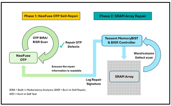
Figure 1. Two-phase approach designed for SRAM repair, based on the integration between NeoFuse OTP and Tessent™ MemoryBIST & BISR Controller.
4. Enables In-Field Incremental Repair for Silicon Lifecycle Management
AI chips operating in data centers under sustained high temperatures are highly susceptible to negative bias temperature instability and hot carrier injection disturbances, causing weak bits present at manufacturing to degrade into hard failures. NeoFuse's high capacity enables incremental repair, endowing chips with resilience throughout their entire lifecycle.
- Non-destructive update: during system maintenance or reboot, MBIST can detect newly developed aging-induced defects. New repair information is written to the incremental blocks reserved in the OTP without overwriting the original factory data.
- Merged loading: during each boot-up, the BISR controller automatically merges original factory data with in-field incremental data, reconfiguring the chip to a zero-defect state.
Conclusion
As Moore’s Law scaling increasingly decouples from cost, power, and yield improvements at advanced nodes, and as generative AI workloads drive unprecedented on-chip SRAM capacity, SRAM yield has become a primary determinant of AI chip profitability. By adopting the integrated solution from eMemory NeoFuse OTP and Siemens’ Tessent™ MemoryBIST, designers can not only dramatically improve 3nm wafer yield to over 90% during manufacturing but also extend chip lifetime and reduce total cost of ownership in data centers through in-field repair mechanisms. This is more than just a memory repair technology; it represents the critical infrastructure supporting the economic viability of advanced process nodes.