
Whilst chiplets garner much interest, many remain cautious about adopting multi-die solutions because the technology transition affects far more than just packaging; it changes the approach to design methodology, verification, manufacturing, and system architecture. However, recognizing the potential payoffs helps explain why the industry continues to advance in measured steps.
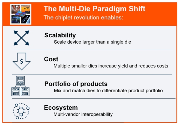
Figure 1: Multi-Die Paradigm Shift (Source: Arteris, Inc)
To confidently adopt chiplet architectures, engineers must solve two core problems involving predictable data movement across dies and manageable system integration. Arteris addresses these challenges through configurable interconnect technology and system-level integration tooling that allow architects to scale designs across multiple silicon domains while maintaining architectural control.
Breaking the Reticle Barrier
At advanced nodes, reticle limits cap die sizes at 26mm by 33mm, or 858 mm². Designs that approach this limit face reduced yield, increasing cost exponentially. Multi-die integration provides an alternative. Rather than pushing a monolithic die size to its limit, architects partition functionality across multiple silicon dies and integrate them within a single package.
Silicon interposers enable aggregate area well beyond a single reticle field. Current implementations reach approximately 80mm by 80mm. Larger interposer formats approaching 100mm by 100mm are emerging, with projections extending toward 120mm by 120mm in future generations. This packaging capability enables system-level scalability without increasing die sizes.
Because die area strongly impacts yield, architects still favor smaller silicon. Reduced die dimensions improve yield characteristics and lower manufacturing risk. Once functionality is partitioned, however, the architectural challenge shifts from physical size to structured connectivity and data movement. At that point, topology becomes the primary architectural decision. To achieve predictability across dies, architects must first address how traffic flows through the multi-die system. Topology and network-on-chip (NoC) interconnect design determine how transactions move, where arbitration occurs, and how latency is managed.
Topology Shapes Multi-Die Systems
In a multi-die system, topology is not simply a physical arrangement. It defines how data moves from die to die across the package. Physical connectivity alone does not establish system behavior. When functionality is distributed across multiple dies, architects must specify how transactions are interpreted, ordered, and completed as they move between dies. The NoC interconnect, whether coherent or non-coherent, governs how transactions are transported and resolved. Without defined system address maps, arbitration, ordering, and routing control, increasing bandwidth alone does not guarantee deterministic system behavior.
Topology directly constrains how the NoC interconnect manages system traffic. The number of links, their placement, and the routing structure directly shape transaction flow across the fabric. Topology also establishes latency domains within the package, influencing how quickly transactions propagate between dies. It determines where arbitration occurs and how bandwidth is allocated across the fabric. As die counts increase, the NoC interconnect must maintain ordering, coherency where required, and traffic isolation across these domains.
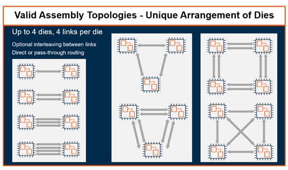
Figure 2: Valid Assembly Topologies – Unique Arrangements of Dies (Source: Arteris, Inc)
Managing Traffic Across Silicon Domains
Multi-die systems introduce hierarchy into what was previously a flat on-die architecture. Each die may contain local memory controllers and defined address regions. Some transactions resolve locally, while others traverse die-to-die links to reach remote memory controllers. This creates a layered model in which traffic may remain within a local die, cross die boundaries to access remote memory, or be routed based on address map resolution decisions. Address maps must explicitly define which regions are local and which are remote. The NoC interconnect fabric interprets those mappings and routes transactions accordingly, creating a non-uniform memory architecture at the package level, with latency higher to remote dies.
Unlike monolithic interconnects, multi-die fabrics must account for additional latency to remote chiplets and die-to-die link bandwidth constraints. Data movement across dies introduces new arbitration points that directly influence system behavior. Scaling, therefore, requires not only wider links but disciplined routing and transaction management within the assembly. Effective multi-die design depends on clearly defined traffic behavior between silicon domains. Architects must determine which requests remain within a local coherency domain and which traverse to remote dies, and how the NoC interconnect applies control at each boundary crossing. These policies control access to memory controllers and direct traffic distribution across the fabric.
As dies are arranged within a package, physical placement introduces additional constraints. Logical port mapping must abstract these physical differences so that routing policies remain consistent regardless of die rotation. Without this abstraction, scaling becomes increasingly constrained as die counts grow. Arteris addresses these requirements through its configurable Ncore coherent interconnect with multi-die support, enabling hierarchical routing and memory visibility across chiplets. For non-coherent and accelerator-centric designs, FlexNoC Interconnect IP and FlexGen Smart Interconnect IP provide configurable fabrics that manage traffic distribution and bandwidth allocation across die boundaries.
In this environment, there is no single interconnect configuration. Each implementation must reflect workload characteristics, memory organization, die count, and placement constraints. Configurability ensures that data movement aligns with overall system architecture, but predictability alone is not sufficient. Multi-die architectures must also support manageable system integration across multiple silicon domains. Chiplet-based solutions may be optimized by simultaneously configuring the entire multi-die device. As dies are combined within a single package, maintaining consistent system definitions, register maps, and interface descriptions becomes a critical integration challenge.
Integration at the Package Level
Partitioning a design across multiple dies introduces integration complexity beyond connectivity. Individual dies may include their own register definitions and machine-readable interface descriptions, while software teams require a unified representation of the complete package device. As dies are combined and connectivity evolves, maintaining consistency across register maps and address spaces becomes increasingly challenging. Integration tooling must consolidate individual die descriptions into a coherent package device-level definition. Arteris Magillem products support this process by consolidating chiplet-level specifications into a single source of truth for the complete multi-die device. From this authoritative representation, unified register maps and IP-XACT descriptions are generated to ensure consistency across hardware and software.
Multi-die integration extends physical limits but also increases system complexity. Once functionality spans multiple silicon domains, transaction behavior can no longer be treated as an implementation detail. It must be intentionally defined within the interconnect fabric.
As reticle limits force designs to partition functionality across multiple dies, success will depend on how effectively architects manage data movement and maintain manageable system integration across silicon domains.
Learn more at arteris.com/multi-die.
 Ashley Stevens is Director of Product Management and Marketing at Arteris responsible for coherent NoCs and die-to-die interconnects. He has over 35 years of industry experience and previously held roles at Arm, SiFive and Acorn Computers. He holds 11 granted patents and has a degree in Computer Engineering from Queen Mary University of London.