
Catalog of SIP Cores
System on Chip design resources
System on Chip design resources
150mm and 200mm wafer fabs account for two-thirds of total closures.
June 16, 2015 -- Since the global economic recession of 2008-2009, the IC industry has been on a mission to pare down older capacity (i.e., ≤200mm wafers) in order to produce devices more cost-effectively on larger wafers. From 2009-2014, semiconductor manufacturers have closed or repurposed 83 wafer fabs, according to data compiled, updated, and now available in IC Insights’ Global Wafer Capacity 2015-2019 report.
Figure 1 shows that 41% of fab closures since 2009 have been 150mm fabs and 27% have been 200mm wafer fabs. Qimonda was the first company to close a 300mm wafer fab after it went out of business in early 2009. More recently, ProMOS and Powerchip closed their respective 300mm wafer fabs in 2013.
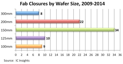
Figure 1
Semiconductor suppliers in Japan have closed 34 wafer fabs since 2009, more than any other country/region over the past six years. In the 2009-2014 timeframe, 25 fabs were closed in North America and 17 were shuttered in Europe (Figure 2).
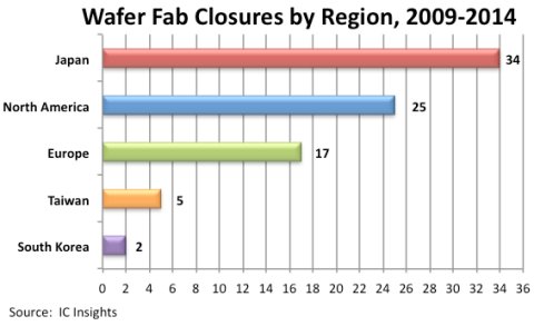
Figure 2
Worldwide fab closures surged in 2009 and 2010 partly as a result of the severe economic recession at the end of the previous decade. A total of 25 fabs were closed in 2009, followed by 24 being shut down in 2010. Ten fabs closed in 2012 and 12 were removed from service in 2013. Six fabs were closed in both 2011 and in 2014, the fewest number of closures per year during the 2009-2014 time span.
Given the flurry of merger and acquisition activity seen in the semiconductor industry recently, the skyrocketing cost of new wafer fabs and manufacturing equipment, and as more IC companies transition to a fab-lite or fabless business model, IC Insights expects the number of fab closures to accelerate in the coming years—a prediction that will likely please foundry suppliers but make semiconductor equipment and material suppliers a little bit nervous.
Report Details: Global Wafer Capacity 2015-2019
IC Insights’ Global Wafer Capacity 2015-2019—Detailed Analysis and Forecast of the IC Industry’s Wafer Fab Capacity report assesses the IC industry’s capacity by wafer size, minimum process geometry, technology type, geographic region, and by device type through 2019. The report also includes detailed profiles of the companies most likely to build 450mm wafer fabs and gives comprehensive specifications on existing wafer fab facilities. Global Wafer Capacity 2015-2019 is priced at $4,290 for an individual user license. A multi-user worldwide corporate license is available for $6,990.