The DTPCI32DC - Dual Clock 32bit PCI Bus Target Interface from Digital Core Design
Bytom, July the 14th, 2016. The DTPCI32DC is a 32-bit target interface which meets all requirements of the PCI 3.0 specification for a target device. It compromises a minimal gate count with a high-bandwidth data transfer. The Core’s main feature is the presence of two clock domains. - They enable flexibility and higher performance as well – says Tomek Krzyzak, VCEO of DCD – When time required for implementation becomes crucial, the DTPCI32DC brings a domain crossing. Saved time can be used for a specific system implementation instead. The user-friendly back-end interface can be very easily and effectively tailored to the design needs.
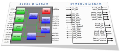
The Core supports up to six Base Address Registers and Expansion ROM address register with both I/O and Memory space decoding from 16 bytes up to 4 GB. Another important feature is a cache wrapping hardware support and a cacheline pre-fetching capability. The DTPCI32DC is accepting size cache lines which are powered from 2 up to 128. It enables also target-disconnect with data, without data or by a target abort. Moreover, the DTPCI32DC is capable to work with 66 MHz clock frequency in the most popular technologies. It assures the PCI timing requirements, as well as other parameters like FIFOs depths number or Base Address Registers (they can be easily configured at the pre-synthesis stage).
More information & evaluation requests: http://dcd.pl/ipcore/1112/dtpci32dc/
Key Features:
- Fully supports PCI specification 3.0 protocol
- Stable clock domain crossing regardless of the clock frequencies
- Cache wrapping (cache lines must be powers of 2)
- User controlled burst data transfer
- Possible no-wait state transactions
- Automatic handling of configuration space read/write access
- Parity generation and parity error detection
- Single interrupt support
- Configurable FIFOs depth
- Supported backend initiated burst termination (with and without data)
- No tri-state buffers
|
Digital Core Design Hot IP
Related News
- DI2CMS, I2C Master - Slave Bus Interface from Digital Core Design
- NewLogic Offers IEEE 802.11 a/b/g CMOS Dual-band WLAN Radio IP with digital Interface
- M31 Announces New 12nm Digital PLL IP to Drive the Benefits of IoT Clock Technology
- Rambus Delivers PCIe 6.0 Interface Subsystem for High-Performance Data Center and AI SoCs
- Enhanced Serial Peripheral Interface (eSPI) Master/Slave Controller
Breaking News
- Ceva multi-protocol wireless IP could simplify IoT MCU and SoC development
- Controversial former Arm China CEO founds RISC-V chip startup
- Fundamental Inventions Enable the Best PPA and Most Portable eFPGA/DSP/SDR/AI IP for Adaptable SoCs
- Cadence and TSMC Collaborate on Wide-Ranging Innovations to Transform System and Semiconductor Design
- Numem at the Design & Reuse IP SoC Silicon Valley 2024
Most Popular
- GUC provides 3DIC ASIC total service package to AI/HPC/Networking customers
- Qualitas Semiconductor Appoints HSRP as its Distributor for the China Markets
- Siemens collaborates with TSMC on design tool certifications for the foundry's newest processes and other enablement milestones
- Credo at TSMC 2024 North America Technology Symposium
- Huawei Mate 60 Pro processor made on SMIC 7nm N+2 process
E-mail This Article | Printer-Friendly Page |