Reliance on existing wafer sizes increases as outlook for 450mm wafers fades.
December 16, 2016 -- IC Insights has just released its new Global Wafer Capacity 2017-2021—Detailed Analysis and Forecast of the IC Industry’s Wafer Fab Capacity report. Shown below is a brief excerpt from that report.
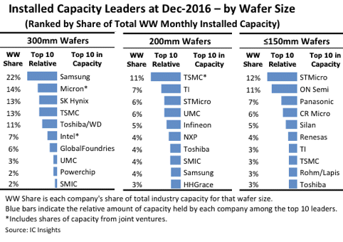
Prior to 2008, the 200mm wafer was used in more cases for manufacturing ICs than any other wafer size. However, since 2008, the majority of IC fabrication has taken place on 300mm wafers. Rankings of IC manufacturers by installed capacity for each of the wafer sizes are shown in Figure 1. The chart also compares in a relative manner the amounts of capacity held by the top 10 leaders.

Figure 1
Looking at the ranking for 300mm wafers, it is not surprising that the list includes only DRAM and NAND flash memory suppliers like Samsung, Micron, SK Hynix, and Toshiba/Western Digital; the world’s five largest pure-play foundries TSMC, GlobalFoundries, UMC, Powerchip, and SMIC; and Intel, the industry’s biggest IC manufacturer (in terms of revenue). These companies offer the types of ICs that benefit most from using the largest wafer size available to best amortize the manufacturing cost per die, and have the means to continue investing large sums of money in new and improved 300mm fab capacity.
The leaders in the 200mm size category consist of pure-play foundries and manufacturers of analog/mixed-signal ICs and microcontrollers.
The ranking for the smaller wafer sizes (i.e., ≤150mm) includes a more diversified group of companies. STMicroelectronics has a huge amount of 150mm wafer capacity at its fab site in Singapore, but the company has been busy converting this production to 200mm wafers. Another STMicroelectronics 150mm fab in Catania, Italy, is also undergoing a conversion to 200mm wafers, with plans for that project to be completed in 2017.
A significant trend regarding the industry’s IC manufacturing base, and a challenging one from the perspective of companies that supply equipment and materials to chip makers, is that as the industry moves IC fabrication onto larger wafers in bigger fabs, the group of IC manufacturers continues to shrink in number (Figure 2).
Today, there are less than half the number of companies that own and operate 300mm wafer fabs than 200mm fabs. Moreover, the distribution of worldwide 300mm wafer capacity among those manufacturers is becoming increasingly top-heavy.

Figure 2
Report Details: Global Wafer Capacity 2017-2021
IC Insights’ new Global Wafer Capacity 2017-2021—Detailed Analysis and Forecast of the IC Industry’s Wafer Fab Capacity report assesses the IC industry’s capacity by wafer size, minimum process geometry, technology type, geographic region, and device type through 2021. The report includes detailed profiles of the companies with the greatest fab capacity and gives comprehensive specifications on existing wafer fab facilities. Global Wafer Capacity 2017-2021 is priced at $4,290 for an individual user license. A multi-user worldwide corporate license is available for $6,990.