
A Practical Guide to PLL Frequency Planning for Modern Systems
1. Introduction
How do you ensure that every part of a system receives the clock it needs—without wasting power or sacrificing performance? The answer lies in creating a well-structured frequency plan built around a PLL.
Many systems use a PLL to generate the main system clock and provide clocks for other subsystems. This article explores how to develop the an effective frequency plan, highlights the trade-offs of different control methods to achieve desired results and uses examples to illustrate the approach.
2. Background – PLL setup
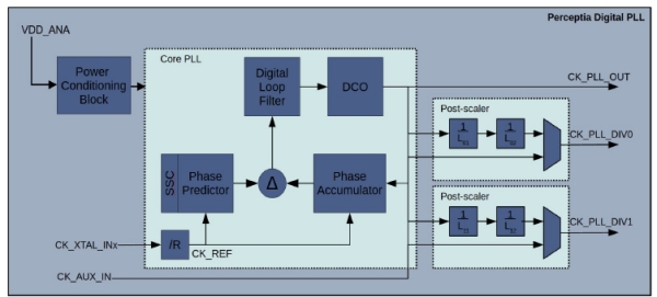
Figure 1: Block Diagram of Perceptia pPLL03
There are several ways to adjust the output frequency of a typical PLL. Figure 1 shows the block diagram of Perceptia’s pPLL03, as an example, highlighting the main control blocks:
- Changing the external reference clock (CK_XTAL_INx).
- Changing the prescaler (/R) to divide CK_XTAL_INx to generate the internal reference clock (CK_REF).
- Changing the PLL multiplier applied to CK_REF in the PLL loop which generates the PLL output clock (CK_PLL_OUT).
- Using integrated postscalers to divide CK_PLL_OUT to generate lower frequency versions (CK_PLL_DIVx).
Each of the above methods can be used to adjust the output frequencies, however, they also introduce different design trade-offs. The potential impacts of using each of these are considered in the next section.
3. Frequency Controls and Their Implications
There are a number of ways to change the output frequency of a PLL. A good frequency plan involves choosing the best combination of these to balance performance and flexibility.
1. Reference Clock Frequency is one factor that sets the output frequency. This can only be changed at design time as the crystal will need to be replaced to change the frequency. The frequency of the reference clock must be within the limits allowed by the PLL datasheet and generally a higher reference clock frequency will lead to lower jitter at the output of the PLL.
| In practice: choose the highest reference frequency the design and PLL allow, but remember this is fixed once the system is built. |
2. The Prescaler is used to divide the input reference clock frequency to an internal reference clock frequency (CK_REF in Figure 1) used by the PLL. This is necessary when the external clock exceeds the maximum CK_REF frequency or when finer output frequency resolution is required – particularly when fractional-N multiplication is not available in a PLL. Be aware that a higher reference clock frequency will lead to lower jitter at the output of the PLL, so it is best to keep the prescaler value as low as possible to maximise the frequency of CK_REF.
| In practice: only use the prescaler when absolutely necessary; lower prescaler divide ratios usually give better jitter performance. |
3. The multiplication ratio determines the main output frequency of the PLL, which is the internal reference clock frequency times the multiplication ratio. The multiplication ratio can be an integer or fractional number depending on the design of the PLL. While fractional-N ratios provide flexibility, jitter performance is generally better with integer ratios—unless the PLL is specifically designed for fractional operation (e.g., Perceptia’s pPLL08).
| In practice: use integer multiplication whenever possible, unless fractional operation is necessary or is explicitly supported for low jitter. |
4. The postscaler divides the main PLL output to create secondary outputs relative to the main output frequency. In the pPLL03 from Figure 1, the frequency of secondary output CK_PLL_DIVn will be the main output frequency divided by LN0, in turn divided by LN1.
| In practice: postscalers are best for generating clean lower-frequency clocks, but not for improving jitter performance. |
4. Frequency Planning
4.1 Planning for a Fixed Output Frequency
This section considers systems that operate at a fixed output frequency or with a small number of frequencies used in different modes. For systems with multiple modes, the same analysis applies to each mode, but a single reference frequency must be chosen that provides the best compromise across all cases.
To create a frequency plan, we start with a list of requirements:
Output requirements can include:
- Reference clock frequency
- Output frequency or frequencies
- Jitter requirements
- Interactions between different clocks
- Application specific requirements
- PLL characteristics
Describing an exact flow to create a frequency plan is difficult as there are so many parameters that can be changed, however this section gives a basic plan that can be modified to suit your situation.
Step 1: Determine the Main PLL Output Frequency
The first step is to determine the main output frequency of the PLL (before postscalers). If there is only a single frequency then this is easy. If there are multiple outputs, select a main frequency from which all others can be derived through division. This frequency is often the highest required output, or a higher multiple that allows all required clocks to be generated.
Step 1A: Consider Integer vs Fractional Division of the Output Clock
If the PLL to be used only supports integer division on its output, then the output frequency must be an integer multiple of all output clocks – this can be determined by calculation. If a common integer multiple does not result in a frequency within the capability of the PLL, then multiple PLLs will be required.
If the PLL supports fractional division of its outputs or there is an external fractional divider available, then there is more flexibility available in choosing the PLL output frequency as the fractional division gives finer resolution when dividing a given frequency. However, fractional division introduces jitter because it works by dithering between two division ratios (e.g., ÷1.5 alternates between ÷1 and ÷2). The effect is smaller as a fraction of the output clock when the integer component of the fractional division ratio is large.
Generally, use integer division for higher-frequency outputs with tight jitter requirements, and reserve fractional division for lower-frequency outputs unless the jitter of the lower-frequency output is a critical constraint.
Step 2: Choose the reference clock and multiplication ratio
The reference clock frequency and the multiplication ratio are now be chosen to achieve the main output frequency. Generally, better performance will be achieved for a higher reference clock frequency and/or an integer multiplication ratio – although this is dependent on the performance of the PLL chosen. An RF PLL, such as Perceptia’s pPLL08 may have minimal performance difference when operating in fractional-N mode compared to integer-N, while a more general purpose PLL such as Perceptia’s pPLL03 or pPLL05 will have a bigger difference in performance between integer-N and fractional-N modes.
Step 3: Account for reference source performance
The performance of the crystal or other reference source will also have a significant effect and this should be chosen carefully. Often, a trade-off between the cost of the crystal and the required performance is made.
Step 4: Use prescalers carefully
Where the available crystal frequencies are limited and a given PLL can only be used in fractional-N mode, the prescaler may need to be used together with the multiplication ratio to achieve the main output frequency. However, extra care needs to be taken when using this approach as reducing the internal reference clock (at the output of the prescaler) will reduce the performance of the PLL.
The prescaler may also be used to reduce the internal reference clock frequency when the external reference clock exceeds the maximum reference clock frequency at which the PLL can operate. Generally, using the minimum prescaler ratio to maximise the internal reference clock, within the allowed bounds, will get the best jitter unless there are other considerations.
See the examples in Section 5.
|
Overall Fixed-frequency planning is about finding the best compromise between reference clock, prescaler, multiplication ratio, and division ratios. Start by choosing the main PLL output frequency, prefer integer division for jitter-sensitive outputs, and maximise the reference clock where possible. Careful selection of the crystal and cautious use of the prescaler can significantly improve system performance. |
4.2 Planning for a Variable Output Frequency
Some systems may require operation across a broad range of output frequencies, with frequent changes. This is typical of an RF system that may need to switch between different channels.
Fractional-N Operation
In RF systems it is generally assumed that the PLL will need to operate in fractional-N mode most of the time, so the PLL must achieve the required performance in this mode.
Frequency standards and output range
In many RF systems, the output frequencies are determined by the communication standard to be used, for example 5G or WiFi which operate dynamically across several frequency bands or must support different regional bands with a single design. As RF PLLs often have a limited output frequency range, the key to making the system work will be to ensure that all required frequencies can be generated, either directly or by dividing the PLL output clock frequency.
Frequency resolution
A key parameter in the frequency plan for such a system is the minimum frequency change required – this is often determined by the required frequency accuracy when transmitting. The RF system will often tune the output frequency to account for inaccuracies in the local crystal oscillator by adjusting the multiplication ratio of the PLL. Hence the resolution of the multiplication ratio – generally expressed as the number of fractional bits is important.
Reference frequency considerations
Since the multiplication ratio cannot be chosen to be a single value, the choice of reference frequency is driven more by the performance of the reference oscillator. It is still generally preferred to use a faster reference clock frequency for better performance.
Please see the example in Section 6 for how a frequency plan for 5G device might be constructed.
5 Fixed Frequency Example
A PLL user needs two output clocks from a Perceptia pPLL05,
- 450MHz to clock a microprocessor
- 12.288MHz to clock the audio subsystem (48kHz × 256)
The reference clock will be 50MHz.
The maximum frequency that pPLL05 can achieve is 1GHz
In order to keep the clock to the microprocessor constant and avoid having to over-constrain the digital to account for the higher of two frequencies when doing a fractional division, we want to use an integer division of the main PLL clock. This limits the main clock to two options: 450MHz or 900MHz (450MHz × 2)
Because it is more important that the audio frequency is exact – so that the users hear good audio reproduction, the fractional multiplication of the PLL will be used to generate a frequency that is slightly lower than 450MHz to allow a more exact audio frequency.
5.1 Fixed Frequency Case 1
If a 450MHz is chosen as main PLL output frequency, then this will be output on the main output of pPLL05 on CK_PLL_OUT. To assist the audio clock, the actual frequency will be 449.85MHz, obtained by multiplying the 50MHz reference clock by 8 + 4084/4096. This is 325ppm slower than the original target of 450MHz.
One of the fractional dividers can be used to generate the 12.288MHz audio clock by dividing 449.85MHz by 36+39/64 to obtain 12.28793MHz. This is 5.5ppm slower than the target 12.288MHz – much less than the error of a standard crystal.
5.2 Fixed Frequency Case 2
Alternately, if 900MHz is chosen as the main PLL output clock. An actual frequency of 899.9MHz can be obtained by multiplying 50MHz by 17 + 4088/4096. This is only 108ppm slower than 900MHz – within the error of most standard crystals.
The 450MHz can then be obtained by using one of the output dividers to divide this clock by 2 to obtain 449.95MHz, preserving the 108ppm error.
The other fractional divider can be used to generate the 12.288MHz audio clock by dividing 899.9MHz by 73+15/64 to obtain 12.28798MHz. This is 1.8ppm slower than the target 12.288MHz – even smaller than the other case and still much less than the error of a standard crystal.
Both cases above are summarised in the following table:
| Reference Frequency (MHz) | Multiplier | Main Output Frequency (MHz) | Divider | Divider Output Frequency (MHz) | Error (ppm) |
| Case 1 | |||||
| 50MHz | 8 + 4084/4096 | 449.85 | 1 | 449.85 | -325 |
| 449.85 | 36 + 39/64 | 12.28793 | -5.5 | ||
| Case 2 | |||||
| 50MHz | 17+4088/4096 | 899.9 | 2 | 449.95 | -108 |
| 899.9 | 73 + 15/64 | 12.28798 | -1.8 | ||
6RF Example
A team wants to build a 5G radio, operating in the Mid and Low bands, and wants the product to operate in the allowed bands in a number of countries. These are listed below, with the frequency bands supported in each country.
| Country/Region | Mid Band | Low Band |
| Australia | n40, n78 | DSS |
| China | n41, n78 | DSS, n28 |
| Europe | n40, n78 | DSS, n28 |
| India | n78 | n28 |
| Japan | n78, n79 | n28 |
Working from the table above, we find the frequencies that are required to cover all the above standards. The architecture used will run the PLL at twice the LO frequency so that a divide by two, generating I and Q clocks can be implemented local to each TX or RX stage. The bands and the required frequency ranges are shown in the table below.
| Band | Uplink Band(MHz) | Downlink Band (MHz) | PLL Frequency (MHz) |
| DSS | DSS reuses LTE bands for 5G. This is beyond the scope of this article and is not considered. | ||
| n28 | 703 – 748 | 758 – 803 | 1406 – 1606 |
| n40 | 2300 – 2400 | 2300 – 2400 | 4600 – 4800 |
| n41 | 2496 – 2690 | 2496 – 2690 | 4992 – 5380 |
| n78 | 3300 – 3800 | 3300 – 3800 | 6600 – 7600 |
| n79 | 4400 – 5000 | 4400 – 5000 | 8800 – 10000 |
The overall frequency range, covering all the bands above is from 1.4GHz to 10GHz.
Perceptia’s pPLL08W covers all of these bands with a lock range from 5.25MHz to 10.6GHz. This will also support DSS in any band below 5GHz. pPLL08W delivers phase noise and spurs that are low enough to support 5G’s demanding requirements across this whole band. In addition the fractional-N multiplication with 24 fractional bits supports dynamic tuning to ensure that the carrier meets the demanding requirements of the 5G standard.
7 Perceptia PLLs
Perceptia Devices is an IP and design services provider, based in Sydney, Australia and Silicon Valley. It is focused on PLLs for RF systems and demanding clocking applications. Perceptia offers a range of PLLs suitable for use in systems with frequency plans similar to those described here.
Perceptia’s pPLL03 is a high performance PLL designed for Performance Computing applications such as microprocessors and AI accelerators. These systems typically have frequency plans similar to those in the examples of Section 5. pPLL03 has:
- Output frequency up to 4GHz
- Period jitter better than 4.2ps peak
- A prescaler that can divide the reference clock input between 1 and 15
- Fractional-N multiplication with 12 fractional bits
- Fractional post scalars with 6 fractional bits
Perceptia’s pPLL05 is an ultra low power PLL designed for applications such as IoT and embedded systems where battery capability is limited. These systems typically have frequency plans similar to those in the examples of Section 5. pPLL05 has:
- Output frequency up to 1GHz
- Power consumption less than 0.77mW (22nm and below)
- A prescaler that can divide the reference clock input between 1 and 15
- Fractional-N multiplication with 12 fractional bits
- Fractional post scalars with 6 fractional bits
Perceptia’s pPLL08 is an RF PLL designed for applications such as WiFi and 5G radios. These systems typically have frequency plans similar to those in the examples of Section 6. pPLL08 has:
- Output frequency up to 10.6GHz
- Less than 200fs RMS jitter, integrated from 12kHz to 20MHz
- A prescaler that can divide the reference clock input between 1 and 15
- Fractional-N multiplication with 24 fractional bits for accurate frequency control
- Integer post scalars
8. About the Author
Julian Jenkins, is the CEO and CTO of Perceptia Devices. As CTO, he is the architect of all of Perceptia’s PLL IP where he been among the pioneers in the development of all digital PLLs. Julian has several US and international patents as a result of this work. He has participated in an impressive list of high-speed analog and mixed-signal ICs that are in commercial production. Feel free to contact Julian if you have questions about this topic.
If you have questions about the topics in this article, feel free to contact us at sales@perceptia.com.