Intel's attempts to get back to the leading-edge in chipmaking and foundry TSMC's steps defining that leading-edge will be on show at this year's International Electron Devices Meeting (IEDM) coming up in December, in San Francisco.
www.eenewsanalog.com, Oct. 08, 2024 –
In a late news paper, researchers from TSMC will unveil the N2 manufacturing process, which is a nominal 2nm process designed for computing in AI, mobile and high-performance computing. In the following paper in the same session Intel engineers will provide details of scaling RibbonFETs, the name Intel gives to its nanosheet transistors.
At the IEDM conference TSMC researchers are expected to report that N2 offers a 15 percent speed gain or 30 percent power reduction at a chip density improved by 15 percent or better compared to its own N3 (3nm nominal) process introduced in 2022.

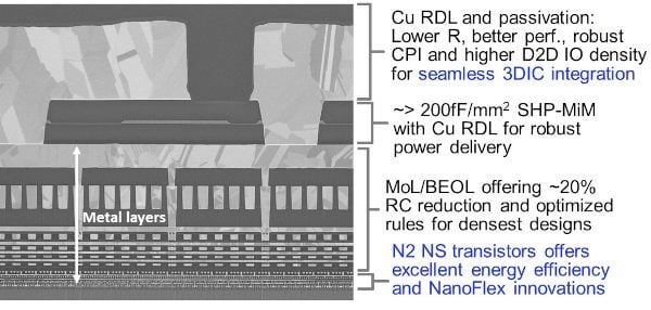
Cross-section of N2 interconnect stack showing copper redistribution layer. Source: IEDM and T the cross-sectional image shows that the N2 platform's Cu redistribution layer (RDL) and passivation provide seamless integration with 3D technologies.
Paper 2.1 2nm Platform Technology Featuring Energy-Efficient Nanosheet Transistors and Interconnects Co-Optimized with 3DIC for AI, HPC and Mobile SoC Applications, authored by G. Yeap et al. from TSMC is also set to show an SRAM macro with a world-record density of 38Mbits per square millimeter.
The paper will also detail middle- (MEOL) and back-end-of-line (BEOL) interconnect that features a scalable copper-based redistribution layer for flexible placement of input/output pads with reduced barrier resistance); a flat passivation layer (for increased reliability); and through-silicon vias, or TSVs (for interconnecting devices in different layers).
The researchers say the N2 platform has met wafer-level reliability requirements and initial qualification tests. Full qualification is expected in 2025 and mass production in 2026.